Clock
prescaler
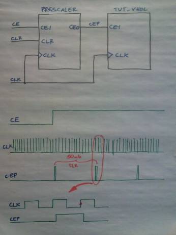
The previous project suffered occasionally from button glitches on clock input. These unwanted events can be removed - instead button driven clock we will use the external generated clock. To do so, we will use 100MHz generator module located on PCB along with a properly built prescaler (i.e. frequency divider), which will mark events for any synchronous modules in our design. To see these events we will slow clock (divide input by 100,000,000) to 1 Hz. Both modules: prescaler and debouncer will be connected in a synchronous way (one and the only clock signal for every flip-flop in the design).
1. Open project from the previous tutorial. Set active the work library tutorvhdl library (context menu Set Active option) . Add the New file Top.bde (Design Browser: Add new file | Block Diagram).
2.
Put on a diagram TutorVHDL module (from the previous lab). Open symbol
toolbox library Symbol Toolbox
(icon ![]() ), find TutorVHDL symbol (in a Project subfolder) and drag
&drop it on the diagram.
), find TutorVHDL symbol (in a Project subfolder) and drag
&drop it on the diagram.
Attn: modul should be succesfully compiled!
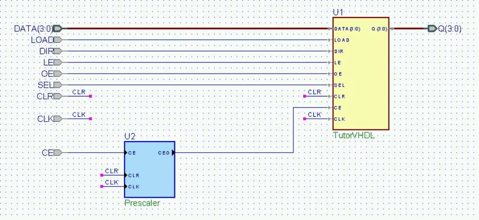
3. Add a Prescaler Fub – draw with a Mouse (context menu - right button). Copy to a C:\My_Designs\TutorVHDL_GGMM\TutorVHDL\src folder Prescaler.vhd file, and then combine it with a Prescaler Fub (context menu Push option). Attn: in pop up window select ‘VHDL Source Code’ and ‘Use existing file’ option.


- Complete your diagram as above – please note that using labels one can improve a diagram readability especially for signals connecting more then two ports
- Read the preskaler module source code. Note the way the
output CEO signal is generated (concurrent assignment with an input CE impact).
Attn: Desired divider is 100.000.000 but first we will start with 10 only. We would like to generally test clock division rather then wait during final simulation (200 millions clock edges to see one tick in our counter TutorVHDL). - Simulate whole project – create TestBench like in previous tasks. Note that you should adjust your input CE, LOAD i DIR signals drivers to 10 times slower clock.
- After successful preskaler module verification enter final division factor value (100.000.000 – and extend the divider register bit length) .
- Set appropriate synthesis options -> select Top-level Unit: Top.
- Modify *.ucf file due to change the
source clock – from button to generator. Add comment character # in a line
#NET "CLK " LOC = "D9"; # BTN<4>
and set 100MHz oscillator active:
## Clock signalNET "clk" LOC = "V10" | IOSTANDARD = "LVCMOS33"; .......Net "clk" TNM_NET = sys_clk_pin;TIMESPEC TS_sys_clk_pin = PERIOD sys_clk_pin 100000 kHz;
Since oscillator is connected to the Global clock buffer line in FPGA on our board the following line:
NET "CLK" CLOCK_DEDICATED_ROUTE = FALSE;
is used no longer and should be commented out or removed.
- Run synthesis and implementation. Configure the circuit and
test in action.
Attn: Select a FPGA proper configuration file top.bit !
Buttons
debouncer
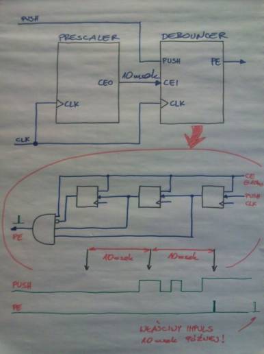
The described above circuit is driven by oscillator – we would like to control CLK action again with a button - but without side effects like push button glitches – so we are going to add another module – debouncer. We can assume that glitches are not longer then 10ms, so we can fetch the push button input and analyse it – any shorter (then 10ms) changes we will dismiss, a longer we will accept. Debouncer module will filter out any glitches on CLK push button and we will stick in our synchronous strategy (one and the only clock signal for every flip-flop in the design). We will add PE signal activating slave modules only due to long term changes on our push button.
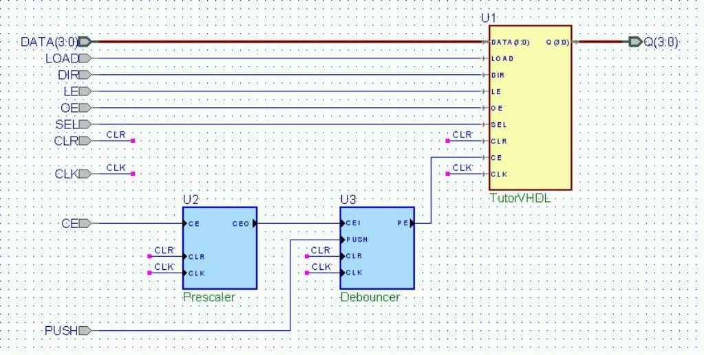
- Complete your diagram as below Add a Debouncer Fub – draw with a Mouse (context menu - right button). Copy to a C:\My_Designs\TutorVHDL_GGMM\TutorVHDL\src folder Debouncer.vhd file, and then combine it with a drawn Fub


- Complete your diagram as above:
- add PUSH port – user button,
- edit Fub, add other ports,
- make necessary connections. - Read debouncer source code. Note the way the output PE signal is generated (concurrent assignment with an input CEI impact).
- Limit dthe division ratio again to 10 to easily observe how it works.
- Simulate the design – modify the TestBench. Add PUSH signal and model some glitches.
- After succesfull verifction, again modify division factor (CEO every 10ms).
- Modify *.ucf file, assign PUSH to BTN<4>:
NET "PUSH" LOC = "D9"; # BTN<4> - Run synthesis and implementation. Configure the circuit and test in action.
- Enjoy and report to a supervisor.