VHDL Tutor
During this tutorial we
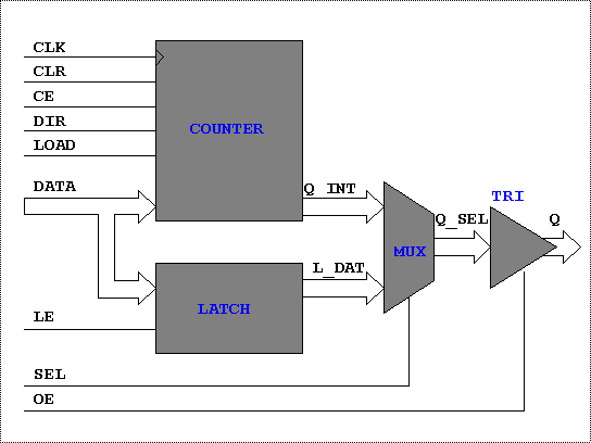
will use VHDL to design a simple circuit with submodules frequently used in
digital designs (with appropriate control signals):
-
synchronous circuitry using
D- type flip flops (for example counter),
-
combinatorial circuitry
(like multiplexer, three state buffers)
-
memory using D-type latches.
Introduction
- Start Active HDL and create the New Workspace
titled „TutorVHDL_DtHHMM”, where Dt is the day of the week (Mon, Tue, Wed,
Thu, Fri) and HHMM is the hour and minute of the lab start for example
„TutorVHDL_Thu1400”).
- Within the new workspace set up an empty
project called TutorVHDL.
- Copy the file TutorVHDL.vhd to the directory
“…\My_Designs\TutorVHDL_GGMM\TutorVHDL\src file\” , then add it to your project
using "Add new file" command (click Add existing file).
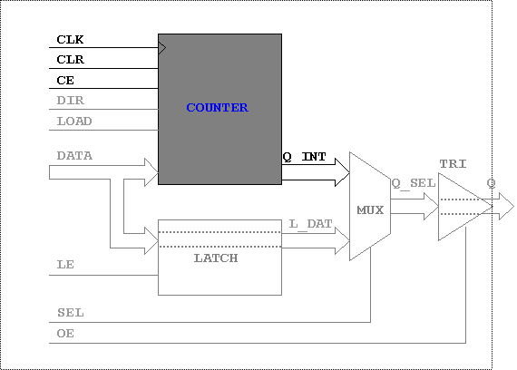
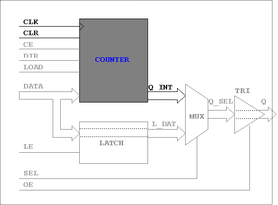
- Look at the src file - it describes 3
bits binary counter, with a synchronous clear input - CLR. Compile the
project.
Tasks
Please note - any change
should be accompanied by appropriate comments in the source code.
To verify your progress make
a functional simulation and prepare/update the testbench.
Task 1. Creating Testbench
-
Open the simulation window
(Waveform Viewer). Select all project's signals (CLK, CLR, and Q) and put them
into a simulation window.
-
Assign stimulators to input
signals: CLK -> Clock (default parameters), CLR -> Hotkey (key 'C' on
your keyboard).
-
Set the simulation step to
100ns, then perform one step of a simulation (“Run For” button - F5), hit
button 'C' to change the CLR signal to 1, then run next simulation step, hit
again 'C' to force CLR signal back to 0, and then run at least 10 steps of
simulation
(until 1200ns). Observe the simulation resuls.
-
Stop the simulation (menu
option Simulation | End Simulation) and save the simulation results to a file
"Initial.awf.
-
Close the timing simulation
window (Waveform Viewer). Please note that you should keep only one active
simulation window.
-
Run the automatic testbench
generation. Testbench files generated at this stage, should be used and
manually upgraded during the next tasks. (menu option Tools | Generate
testbench).
-
Select the right entity
(tutorvhdl) and select the Single Process testbench Type.
-
In the next window, select
the check test vectors from file and point to the Initial.awf file with
previously stored simulation results.
-
If file reading is OK all
UUT (Unit Under Test) signals should be properly assigned to values read from
file.
-
In the next stage, agree
with the proposed names generated by the testbench wizzard.
-
DO NOT select the option to
generate the configuration for the simulation time (timing simulation).
-
Run the testbench macro
tutorvhdl_TB_runtest.do created in the
TB folder (context menu (right mouse button) click Execute.)
-
Observe the testbench
results (should correspond to the previous ad hoc simulation)
Task 2 Change Q_INT variable into a Q_INT Signal
-
Remove variable definition
from the process statement.
-
Define local Q_INT signal
for your architecture
-
Change the assignment
operator ("<=" instead ":=")
-
Ensure that the system still
works correctly - check if output changes on the rising edge of the clock ( if
not, explain why?)
-
Move the Q_INT signal
assignment out of the process instruction - observe results
Task 3 Change CLR signal from synchronous to
asynchronous
-
Edit the Testbench file to
ensure that CLR signal changes out of
the CLK slopes - just to show the asynchronous behaviour.
-
Move the “if CLR …..” test
VHDL line ahead of detecting CLK rising edge VHDL code
-
Upgrade the process
sensivity list.
-
Show the proper simulation
results with asynchronous CLR to the supervisor.
Task 4 Decimal counter
-
Change the binary counter
(3 bits) to decimal counter (0...9). Note that you should extend the width of
the vector objects in the whole project ( not only the source file but the
Testbench as well)
-
Use convenient vector
signal assignment Q_INT <= (others => '0 ') instead of: Q_INT <=
("0000").
-
Extend the simulation time
– in the Testbench file
-
….
-
wait for 1825ns;
-
END_SIM <= TRUE;
-
...
-
Extend the simulation time
in a macro *.do
-
...
-
run 2000ns;
When END_SIM flag is used,
you can use only run command (without the time limit) in a macro *.do.
Simulation time will be controlled in just one Testbench file this way.
Task 5 Clock enable control pin
-
Enter the input signal CE,
unlock (high state) synchronous counter operations. Construction:
…
if CE = '1 'then
…
end if;
should be inserted properly inside the clock detection
clause (why?).
-
Upgrade Testbench file:
o
component UUT signals
declaration section
o
local signals declaration
section for TB architecture
o
local signals mapping
o
main TB process should assign
values to a new signal
-
Upgrade macro *.do
o add command to monitor introduced signal to the timing simulation (Waveform Viewer):
...
wave-noreg
CE
The next tasks require
similar TB upgrading – the new circuit features should be clearly shown in simulation
– so TB modifications should add successive test vectors to the existing ones,
rather than replacing them.
Task 6 Loadable counter
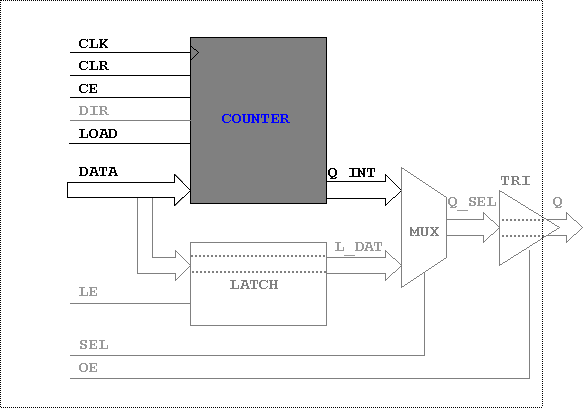
Change our counter into the loadable one - add the LOAD input – it should work synchronously. Add the appropriate input data bus DATA – when the LOAD input is active (say high) the counter output should copy the DATA bus to its output, when LOAD goes low counter should start count from loaded value.
Task 7 Reverse counter
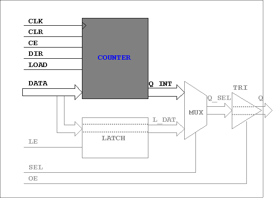
Upgrade the counter to
reverse counter – add the DIR input to control the counting direction.
Task 8 Multiplexer
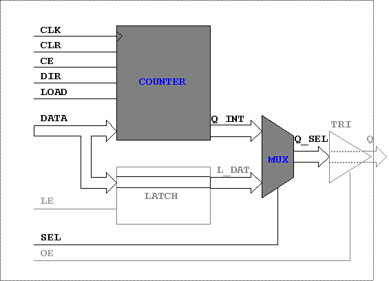
Add the multiplexer
controlled by signal SEL. When SEL input is active (say high) the multiplexer
output should copy the counter output Q otherwise a module output should copy
the data bus (DATA). Use the concurrent signal assignment.
Task 9 Three state buffer
Add the three state buffer
at the circuit output, controlled by input signal OE.

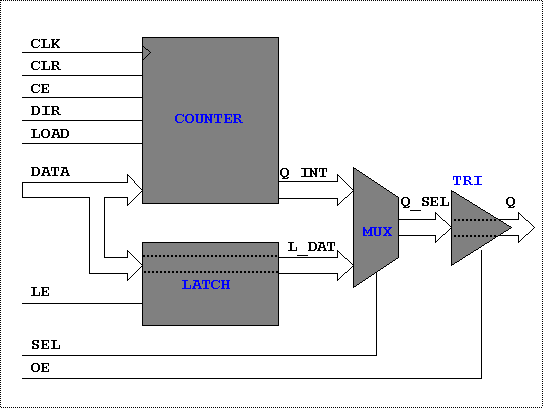
Task 10 Latch
Add the DATA latch signal –
input LE activated, to hold the input data (DATA) before being placed to the
multiplexer input.
